A 22-Gb/s Time-Interleaved Low-Power Optical Receiver With a Two-Bit Integrating Front End
This is a novel 22-Gb/s energy-efficient optoelectronic receiver architecture in 65-nm CMOS for short-reach optical communication. The receiver incorporates four sub receivers with a two-bit integrating resettable front-end in each sub receiver. The two-bit integrating low-bandwidth front end replaces the full-bandwidth transimpedance amplifier used in conventional optoelectronic receivers, resulting in improved energy efficiency. The low-bandwidth operation is enabled by using a capacitor at the input and by amplifying the two-bit integrated voltage with low-bandwidth voltage gain stages that require a bandwidth of only 35% of the operating data rate. The receiver performs a 1:4 demultiplexing operation by only using two quarter-rate clock phases instead of the four phases that are conventionally used in a quarter-rate clocking system. This clocking scheme reduces complexity while maintaining the same timing margin of the quarter-rate systems. This two-clock phase system is enabled by optical delay lines and splitters. The receiver is experimentally validated with a 1550-nm photodetector array wire bonded to the four inputs. The electronic part of the receiver achieves error-free transmission (BER < 10^-12) at 22 Gb/s with an energy efficiency of 1.43 pJ/bit and an average sensitivity of -7.8 dBm (or -6.2 dBm optically modulated amplitude) with a 1.09-V supply.
Read about this receiver in my paper here.
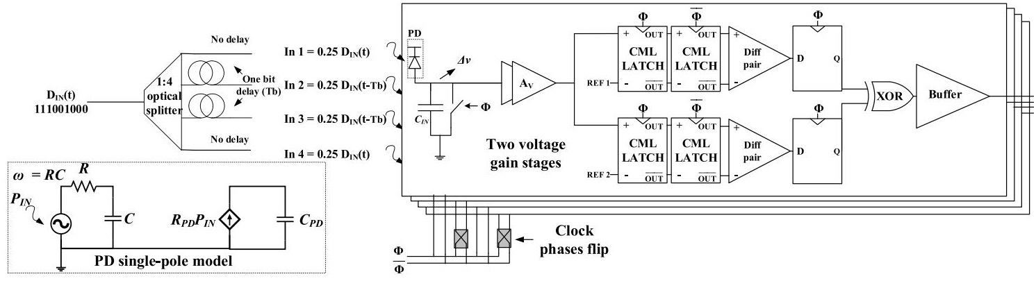
Receiver block diagram.
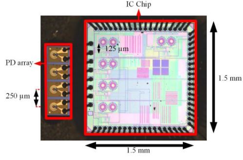
IC micrograph.
A 17 Gbps 156 fJ/bit Two-Channel Optical Receiver With Optical-Input Split and Delay in 65 nm CMOS
Multi-channel optical receivers clocked at a frequency slower than the data-rate in which different phases are used for each channel are widely used in high data-rate applications. Here, we demonstrate a two-channel optical receiver where both channels share the same clock operating at half of the data-rate frequency. However, instead of using different phases for each channel, the optical input is split and the input to the 2nd channel is optically delayed with respect to the 1 st channel. Moreover, to improve performance, the duty cycle of the clock can easily become a design parameter. Each channel consists of only one high-bandwidth gain-improved transimpedance amplifier with a pseudo-differential-output and a comparator with offset-nulling. The receiver is fabricated in 65 nm CMOS. To demonstrate the concept, the fabricated die and two photodetectors are bonded inside a QFN80 package. Measurement results of the receiver show that each channel can sample the input at 8.5 Gbps, resulting in a 17 Gbps total data rate, with a superior energy efficiency of 156 fJ/bit , and an input optical modulation amplitude (OMA) sensitivity of -7 dBm without any equalization.
Read about this receiver in my paper here: PDF LINK
LINK
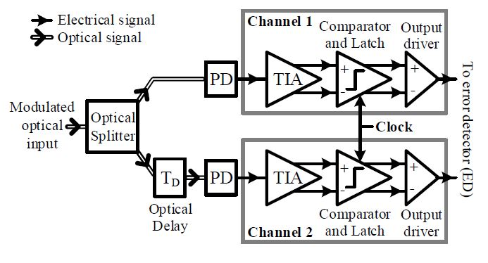
Receiver block diagram.
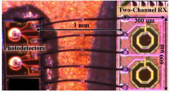
IC micrograph.
An RF antenna in silicon photonics
I design and measure a 15 GHz monopole antenna implemented in silicon photonics for inter-chip communication in this project. The antenna is designed in HFSS with its radiation pattern simulated. To confirm its operation and experimentally demonstrate inter-chip communication, the antenna is fabricated in a commercial Silicon Photonics fabrication process. Measurements include s-parameter using a vector network analyzer, and inter-chip data transmission between two on-chip antennas. The inter-chip data transmission is demonstrated using an off-chip photodetector directly as a transmitter as a proof-of-concept. Results indicate the feasibility of a monolithically integrated photodiode-antenna system as a transmitter.
Read about this antenna in my paper here.
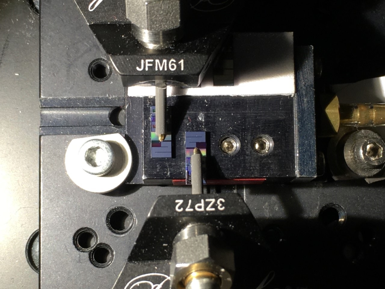
Antenna measurments testbed.
Optical Receiver Exploiting Silicon Photonic Delay Lines for Clock Phases Generation Replacement
This project aims to design a high-speed optoelectronic receiver in 65 nm CMOS technology. The receiver utilizes only two clock phases instead of the four conventionally used in a quarter-rate clocking system. This two-clock phase system is enabled by a passive silicon photonic split and delay structure that eliminates the need for a quadrature clock phase generator and all the associated buffers. Moreover, the outputs of the receiver are demultiplexed which further helps reducing power consumption in the digital part of the system. The receiver also employs inter-stage AC coupling and is mounted on a high-speed printed circuit board (PCB). The impact of AC coupling and PCB parasitics is investigated. The functionality of the receiver is validated by highspeed optical measurements. The receiver achieves an error-free transmission up to a data rate of 12.5 Gb/s with an energy efficiency of 1.93 pJ/bit and a sensitivity of -4 dBm from a 1 V supply.
Read about this receiver in my paper here.
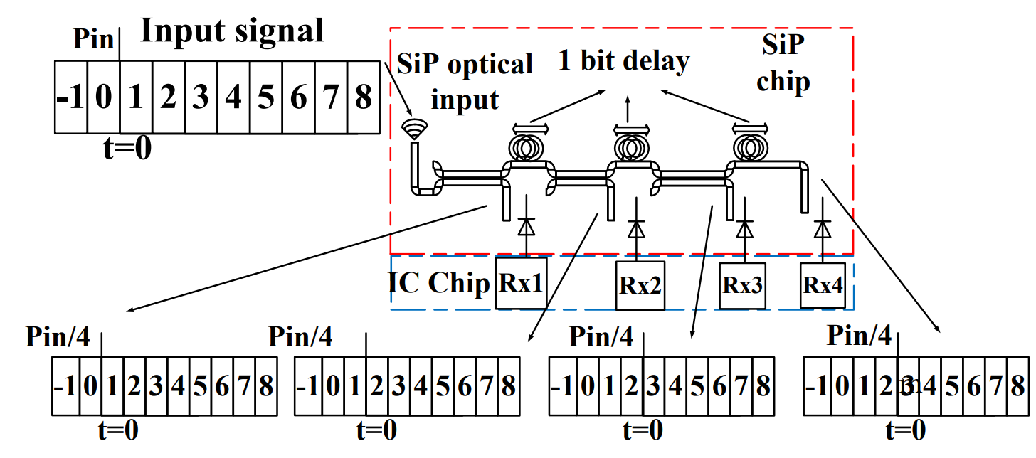
Principle of operation
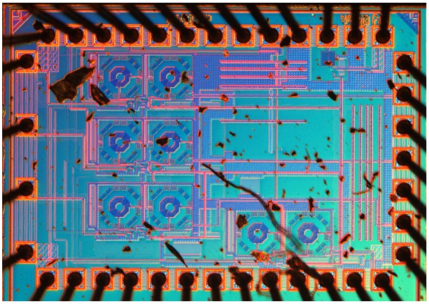
Micrograph of the IC chip